PCB Manual Placement Helper in HTML
This is the first real post, so I’ll start with a very small “Hello World” thing.
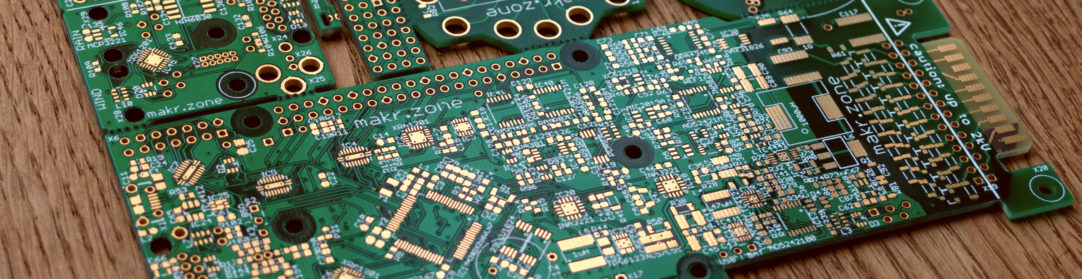
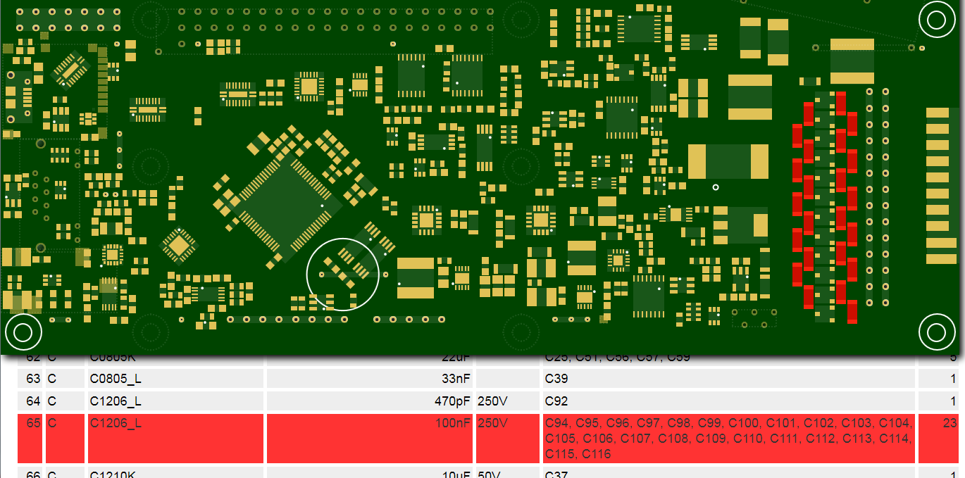
I’m currently manually placing quite complex PCBs using this cartesian guide:
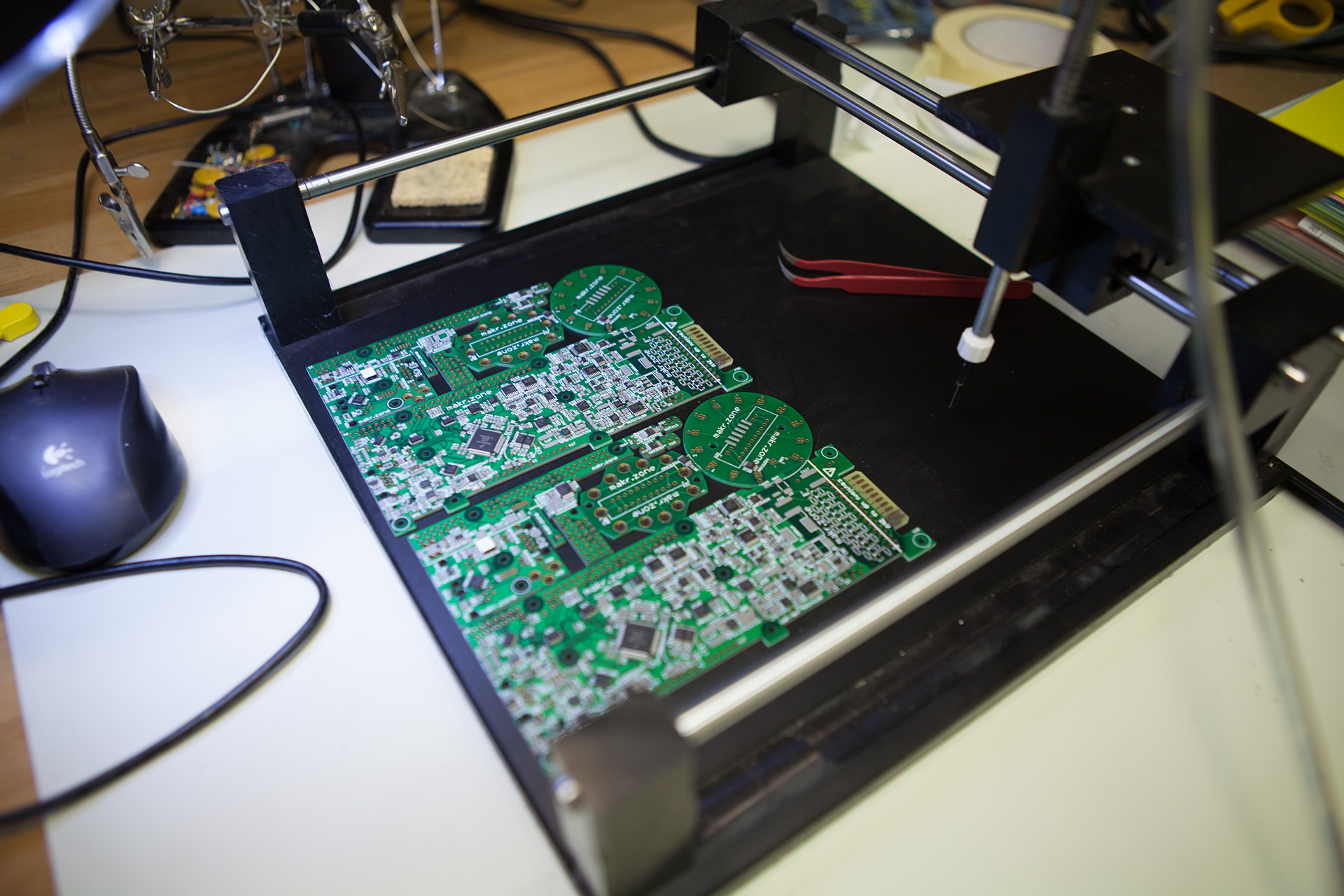
As an example, the last PCB revision (pictured above) had ~120 different SMD parts, ~400 in total. I chose to assemble two boards. It took me ~10 hours (!) to assemble the boards even with a friend helping, sorting out the parts on the go. So comparing this to some reports on forums, I must be quite clumsy at it. My presbyopia doesn’t help.
I’m using EAGLE™ 7.x and (to my astonishment) I was unable to find a practical solution to help me pinpoint and place the parts on the rather dense PCB. So I quickly rolled my own little helper in HTML.
It does the job for me but it’s very minimalist, don’t expect too much!
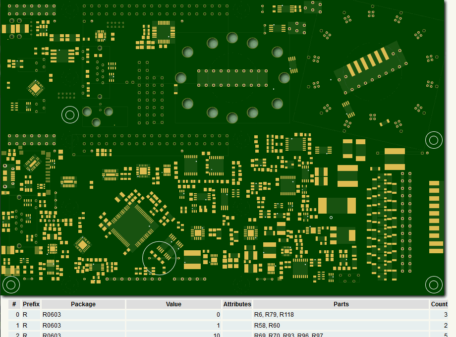
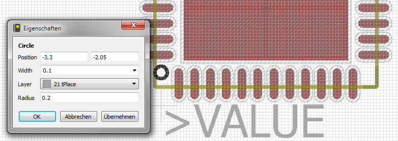
The PCB rendering
The HTML—or rather the embedded script—kind-of draws the board by showing pads (through holes) and smds (solder lands). A bounding box of the footprint is slightly highlighted. All silk screen layer circles are drawn to show you the typical “pin 1” markers. That’s it. You need to use the browser’s zooming to adjust the size.
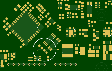
It only offers a top view for smd and through holes. If you have “pin 1” markers other than circles it won’t work. You have to change your packages (or smarten up the script).
The parts list
Underneath is a scrollable list of the parts. You can click on a line and the corresponding parts are highlighted in red on the board. You can also click on a part on the PCB and it will scroll to this line and highlight it in turn.
Usage
Just download the github files into a folder. Did I say it’s minimalistic? No fancy file selection dialog, you need copy your .brd file, rename it to “board.brd”, then place it side by side with the .xhtml into the folder. Then just open the .xhtml and be patient for a sec or two, the embedded script takes some time to parse the .brd xml and render.
NOTE: Newer browsers might require a security setting to allow this, see the discussion here.
Some internals
All rendering is done using straight HTML+CSS, no fancy SVG or similar. I wanted it to be supported on old/simple devices/browsers.
I originally wanted to project the image onto the PCB using a little LED projector (never found the time to set it up though). This should explain why the PCB rendering occupies most of the screen estate and is fixed to the top left corner with no title bar etc., while the parts list somewhat strangely scrolls underneath it.
I’ve developed and used it with EAGLE version 7.x. Have yet to upgrade to version 8 and see if the .brd XML format has changed.
Tweaking
If you want to change the way parts are sorted and grouped, you have to go into the HTML code. There are two notable variables that can be tweaked (look for the beginning of the <script> section):
   <script >
   <![CDATA[

     // sets the priority prefixes and their sort order (others are sorted alphabetically)
     var priorityPrefixes = [ 'R', 'C', 'D', 'L', 'D', 'Q', 'IC' ].reverse();
     // attributes to be considered
     var groupingAttributes = [ 'precision', 'voltage', 'esr' ];
The parts are sorted by package first. But you can override the sorting for some of the package prefixes. I chose to place all resistors first, then caps, then diodes, etc. see the priorityPrefixes array.
All parts with the same package, value and distinct combination of groupingAttributes, are grouped into one line.
The code
Please go to the github repository (this is also my first github project, so if I’m doing this the wrong way, please holler):
All comments, questions etc. welcome!
Also because I’m not a native English speaker, I’m grateful for all language related feedback as well.
Leave a Reply